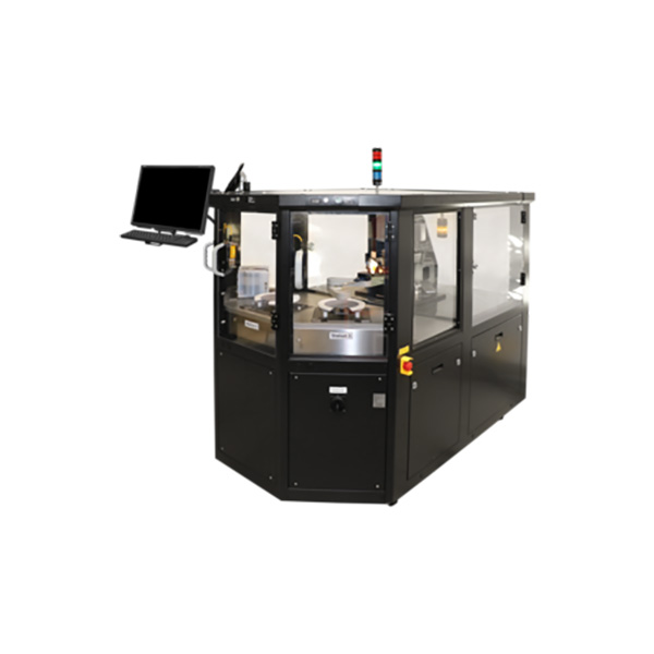
The characteristics of wafer XRD:
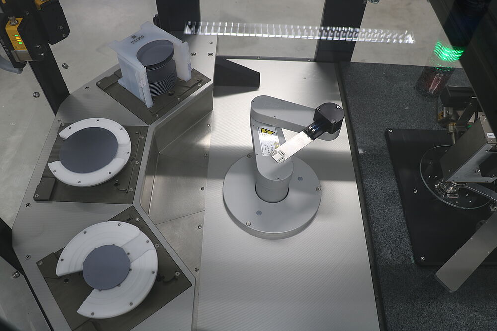
◇A fully automated wafer processing and classification system (e.g. box to box).
◇Measurement of crystal orientation and electrical resistivity
◇Optical determination of geometric features of chips (notch position, notch depth, notch opening angle, diameter, planar position, and planar length)
◇Measurement of distance between unpolished wafers and mirror surfaces
◇MES and/or SECS/GEM interfaces
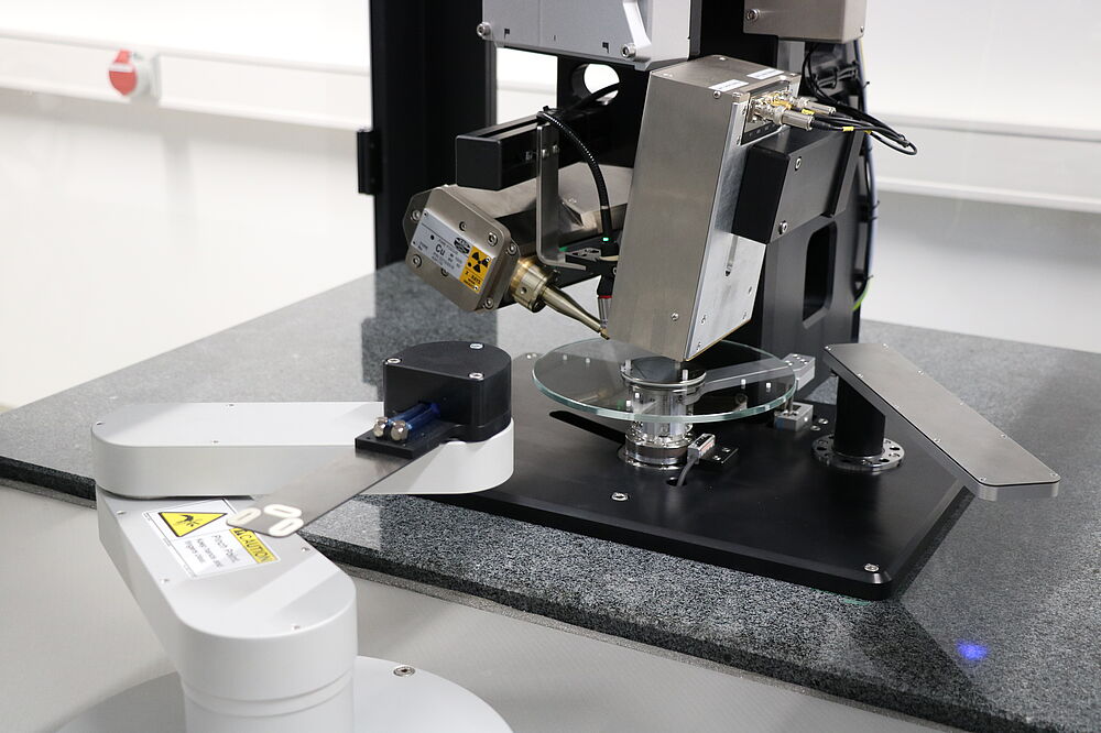
Unique Omega scan method:
◇High precision
◇Measurement speed:<5 seconds/sample
◇Easy to integrate into the production line
◇Typical standard deviation inclination (e.g. Si 100):<0.003 °, less than<0.001 °.
For more information, please contact us.