Product
Current location: Home Product New Energy XRM
  • Three dimensional X-ray microscope (XRM) SKYSCAN 2214 CMOS version
  • Three dimensional X-ray microscope (XRM) SKYSCAN 2214 CMOS version
  • Three dimensional X-ray microscope (XRM) SKYSCAN 2214 CMOS version
  • Three dimensional X-ray microscope (XRM) SKYSCAN 2214 CMOS version
  • Three dimensional X-ray microscope (XRM) SKYSCAN 2214 CMOS version
  • Three dimensional X-ray microscope (XRM) SKYSCAN 2214 CMOS version
  • Three dimensional X-ray microscope (XRM) SKYSCAN 2214 CMOS version
  • Three dimensional X-ray microscope (XRM) SKYSCAN 2214 CMOS version

Three dimensional X-ray microscope (XRM) SKYSCAN 2214 CMOS version

SKYSCAN2214 CMOS version is a new generation of nanoscale three-dimensional X-ray microscope (XRM) launched by Bruker. In addition to retaining the advanced performance of the previous generation SKYSCAN2214<500nm, such as true three-dimensional spatial resolution and multi detector configuration (no more than 4), the device has been upgraded in many aspects in terms of X-ray source power and detector type to ensure that users can obtain a larger imaging field of vision and brighter image data.

Brand: Brooke

Model: SKYSCAN 2214

Minimum order quantity: 1

Unit: Unit

Packaging instructions: Standard shipping packaging

DetailsApplicationParameter

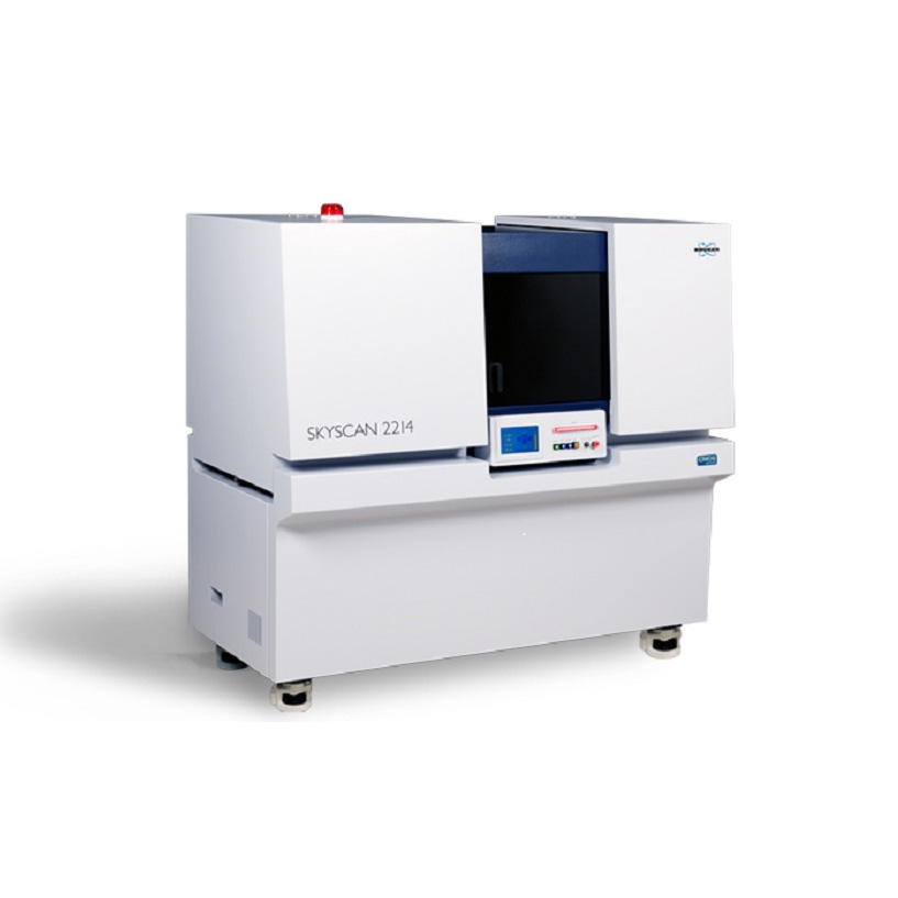
SKYSCAN 2214 CMOS Edition- Multi range nanoscale 3DXX-ray microscope    

The multi-range nanoscale 3D X-ray microscope SKYSCAN 2214 CMOS covers a wide range of object sizes and spatial resolutions, enabling advanced 3D imaging and precise modeling of geological materials, composite materials, lithium batteries, fuel cells, electronic components, and in vitro preclinical applications such as lung imaging or * * vascularization in oil and gas exploration.
   

This instrument can scan and reconstruct the internal microstructure of objects with a diameter greater than 300 millimeters in 3D non-destructive testing, as well as perform sub micron level resolution on small samples.    

In addition, the system is equipped with an "open" transmission X-ray source with a size of<0.5 microns and a diamond window. It can accommodate four X-ray detectors and has great flexibility. Automatic variable acquisition geometry and phase contrast enhancement can achieve excellent quality in a relatively short scanning time.    

SKYSCAN 2214 CMOS will provide users with a complete set of 3D Suits software packages for free. This software suite covers all the functions required by users, including GPU accelerated reconstruction, 2D/3D morphological analysis, and surface and volume rendering visualization. And the software suite can be upgraded for free.     


Main features:
   

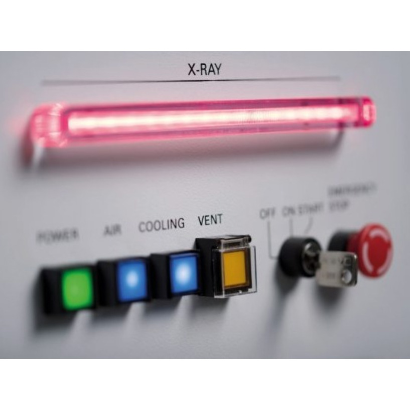
● X-ray light source
   

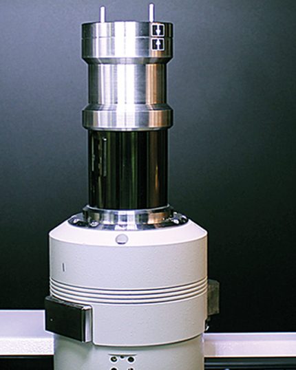
SKYSCAN 2214 adopts a new generation of open X-light sources. This light source can achieve actual spatial resolution better than 500 nm, up to 160 keV X-ray energy, and up to 16 W power. Due to its extremely simple pre registered filament replacement program, this light source requires almost no maintenance.    

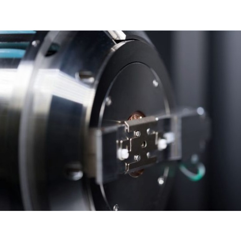
SKYSCAN 2214 features an open (pump type) nanofocal X-ray source with a diamond window. It can generate X-beams with peak energies ranging from 20 kV to 160 keV and provides two types of cathodes. Tungsten (W) cathode is suitable for a complete acceleration voltage range of up to 160 kV, with small spot sizes up to 800 nm. The LaB6 cathode is suitable for accelerating voltages from 20 kV to 100 kV, and the spot size of the X-ray beam can be less than 500 nm, ensuring high resolution in imaging and 3D reconstruction. The JIMA resolution test card shows that it can easily resolve structures up to 500 nm. In order to ensure the long-term stability of the focal spot size and the position of the emission source, the X light source can also be equipped with a water cooling system, which includes a circulation device that can accurately control the temperature of the cooling liquid to maintain temperature stability.     
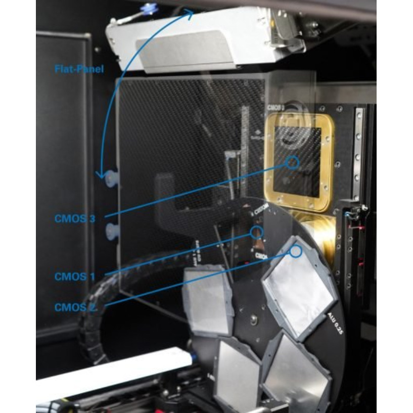


● Detectors    

SKYSCAN 2214 can be equipped with four X-ray detectors for great flexibility: including three scientific and sCMOS detectors with different resolutions and field of view balance, as well as one flat panel detector to cover a super large field of view. Users only need to click the mouse to switch between detectors at will.
   

The use of small pixel large-sized CMOS detectors can extend high-resolution 3D imaging to large objects. The flexibility of the built-in detector allows it to adjust the field of view and spatial resolution based on the size and density of the object. Advanced reconstruction from the volume of interest, allowing for local high-resolution scanning of selected parts of large objects without affecting image quality.    

In addition, by using offset detector positions and vertical object movement, the horizontal and vertical fields of view can be increased, respectively. Afterwards, 3D SUITE software automatically concatenates different images together and accurately compensates for offset and possible intensity differences.    

With the development of research topics and analysis needs, detectors can be upgraded on-site at any time during the system's lifespan.     


● In situ experimental platform

The SKYSCAN 2214 CMOS Edition has a highly accurate sample stage that supports objects with a diameter of up to 300 mm and a weight of up to 20 kg. The air suspended rotary motor can accurately rotate the position of an object with very high accuracy, and the integrated precision positioning platform ensures complete alignment of the sample.

The SKYSCAN 2214 CMOS Edition has a large and user-friendly sample chamber, making it easy to scan large objects and install optional test benches. It has enough space to accommodate peripheral devices such as in-situ testing benches.

Bruker's material testing bench can perform compression tests of 4400 N and tensile tests of 440 N. All test benches can be automatically connected together through the system's rotary table without the need for any external cables. By using the provided software, a scheduled scanning test can be set up.

Brooke's heating and cooling stages can reach temperatures of 80 º C or 30 º C lower than ambient temperature. Like other test benches, the heating and cooling benches do not require any additional connections, and the system can automatically identify different test benches. By using heating and cooling stages, samples can be tested under non environmental conditions to evaluate the effect of temperature on the microstructure of the samples.

The SKYSCAN 2214 CMOS Edition is fully compatible with the DEBEN test bench. With the built-in adapter, the DEBEN test bench can be easily installed on the rotary table of SKYSCAN 2214.


High and low temperature in-situ test bench                            

Mechanical tensile/compressive in-situ testing bench                

Compatible with Deben sample stage            

SkyScan2214 CMOS application instance

Additive manufacturing

Additive manufacturing, also known as 3D printing, can be used to manufacture components with complex internal and external structures. Unlike traditional technologies that require special molds or tools, additive manufacturing can be used to economically produce individual product prototypes as well as to produce large quantities of components. After production is completed, in order to ensure that the performance of the produced components meets expectations, it is necessary to verify the internal and external structures. XRM can perform this type of testing in a non-destructive manner, ensuring that the produced components meet or exceed the specified performance.

◇ Check for internal voids formed by residual powder

◇ Verify internal and external dimensions

◇ Direct comparison with CAD models

◇ Analyze components composed of a single material and multiple materials


Fiber and composite materials

By combining materials into composite materials, the resulting components can have higher strength while significantly reducing weight. To further optimize component performance, it is necessary to ensure that the direction of the components can be optimized. One of the commonly used components is fibers, including steel bars in concrete, glass fibers in electronic components, and carbon nanotubes in aviation materials. XRM can be used to detect fibers and composite materials without the need for cross cutting, ensuring that the sample state is not affected during the sample preparation process.

◇ Direction of embedded objects

Quantitative analysis of layer thickness, fiber size, and spacing

◇ Using an in-situ sample stage to detect temperature and physical properties


geology


Studying geological samples - whether they are core samples from deep underground or rocks above the ground - can provide rich information for exploring the formation process of our world. When analyzing, it is usually necessary to destroy the original sample and eliminate the important origin of the internal structure. XRM can analyze samples without the need for slicing, resulting in faster results and allowing samples to continue to be used for analysis in the future.

Visualize the internal structure of the sample in three dimensions based on density

Visualization of pore networks

Digital slicing allows the use of standard geological analysis methods


Skyscan2214 CMOS Technical Parameters

feature

parameter

advantage

X-ray source

20-160 kW

And 16 W

User replaceable filaments

Optimized to achieve high energy (W) or high resolution (LaB6)

The rotatable diamond window can achieve a long service life

X-ray detector

6 Mp active pixel tablet

16 Mp large-sized CMOS

16 megapixel medium frame CMOS

15 Mp High Pixel CMOS

Different pixel sizes and detector sizes facilitate a balance between detector resolution, coverage range, and counting statistics

Can provide 1, 2, 3, or 4 detectors

Allow on-site upgrades to add detectors

Image format

Up to 8000 x 8000 x 2300 pixels after a single scan

Due to allowing users to choose image sizes, it is possible to balance the size of the dataset with the required resolution.

The software can streamline the collected data

spatial resolution

60 nm pixel size
<500 nm low contrast resolution (10% MTF)

Simple graphical control enables optimization of experimental resolution based on selected detectors, samples, and detector distances.

Adjust the focal spot size of the light source to balance high power and resolution

positioning accuracy

The rotation accuracy is better than 50 nm,
Shockproof granite platform with pneumatic adjustment

The air suspended sample stage allows for smooth rotation of the sample stage

The sample stage can be installed using a simple chuck installation method

Mechanical and electrical interfaces enable it to be used as an advanced material research platform

Object size

300mm diameter (140mm scanning size)

Length 400 millimeters

Object weight 20 kg

Having the energy and space to scan large-sized samples

Small samples can be accurately positioned near the light source to achieve maximum magnification

Equipment size 1800 mm x 950 mm x 1680 mm (width x depth x height)
 
Weight: 1500 thousand

Efficient design can optimize the utilization of laboratory space

Large chain sliding doors facilitate light source maintenance