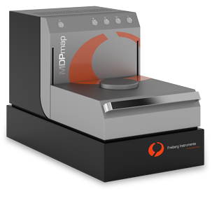
MDPmap:
Single crystal and polycrystalline silicon wafer life measurement equipment for complex material research and development.
Features:
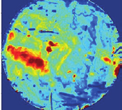
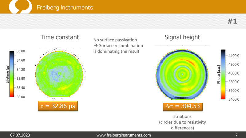
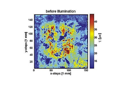
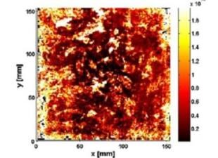
◇Sensitivity: High sensitivity, used to visualize invisible defects to date and investigate the situation of epitaxial layers
◇ Measurement speed: 6-inch silicon wafer<5min, resolution of 1mm
◇ Lifetime range: 20ns to tens of ms
◇ Pollution measurement: Metal (iron) pollution from crucibles and equipment
◇ Measurement ability: From cut silicon wafers to fully processed samples
◇ Flexibility: The fixed measuring head can be connected to an external laser and triggered
◇ Reliability: Modular and compact desktop instruments, higher reliability, with normal operating time>99%
◇ Repeatability:>99%
◇ Resistivity: resistivity mapping, no need for frequent calibration
Technical specifications:
| Sample size |
Diameter up to 300mm (standard table), diameter up to 450mm (customized), * small to 5 x 5mm |
| Life measurement range |
20ns to tens of ms or more |
| resistivity |
0.2->10 ³ Ω · cm, p-type/n-type |
| Sample materials |
Silicon wafers, epitaxial layers, partially or completely processed silicon wafers, compound semiconductors, and more materials |
| Measurable characteristics |
Lifespan- μ- PCD/MDP (QSS), optical conductivity |
| Excitation wavelength |
Choose four different wavelengths from 355nm to 1480nm. 980nm (default) |
| Size specifications |
Volume: 680 x 380 x 450 mm; Weight: approximately 65 kilograms |
| source |
100-250V, 50/60 Hz, 5 A |
Details:
◇
Used for research and development or production monitoring
Flexible surveying and mapping tools
◇MDPmap is designed as a compact desktop non-contact electrical characterization tool for offline production control or research and development, under steady-state or short pulse excitation( μ- Under PCD, measure parameters such as carrier lifetime, optical conductivity, resistivity, and defect information over a wide injection range. Automated sample identification and parameter settings allow for easy adaptation to a variety of different samples, including epitaxial layers and wafers that have undergone different preparation stages, from native wafers to up to 95% metallized wafers.
◇The main advantage of MDPmap is its high flexibility, for example, it allows for the integration of up to four lasers to measure the lifetime of injection levels from low to high, or to extract depth information by using different laser wavelengths. Including bias light facilities, and μ-Option for PCD or steady-state injection conditions. Different maps can be used for customer defined calculations, and main data can be output for further evaluation. For standard measurement tasks, predefined standards only require the press of a button to perform routine measurements.
Additional options:
◇Changes in spot size
◇Electrical resistivity measurement (wafer)
◇Block resistance
◇Background/Polarization
◇Reflection measurement (MDP)
◇LBIC (diffusion length measurement) of solar cells
◇Bias MDP
◇Reference wafer
◇Internal/External Iron Diagram of Silicon
◇Integrated heating table
◇Flexible laser configuration