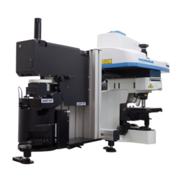
AFM Raman coupling configuration
HORIBA Scientific Raman technology can be coupled with scanning probe microscopy (SPM) to construct a powerful and flexible AFM Raman platform. Researchers can choose appropriate instruments based on the expected AFM Raman working mode.
All configurations equipped with laser scanning technology can quickly image the laser reflection on the scanning probe or image hotspots based on needle tip enhanced Raman scattering signals, thus accurately and reliably positioning the laser onto the SPM probe tip.
The high-throughput optical signal collection and detection hardware ensures the collection of SPM signals and Raman spectra at each point while fast scanning.
Integrate all your requirements into a powerful system
The perfect solution we provide uses direct optical path coupling and optimizes it to achieve high flux. This platform can couple atomic force microscopy (AFM), near-field optical technology (SNOM, NSOM), scanning tunneling microscopy (STM), and confocal optical spectroscopy (Raman and fluorescence imaging) into a multifunctional instrument to achieve needle enhanced Raman scattering (TERS) or confocal measurement.
Combining Nanoimaging and Chemical Analysis

Coplanar AFM and Raman imaging of single-layer, double-layer, and three-layer graphene
- AFM and other SPM technologies can provide morphology, mechanics, thermal energy, electromagnetic field, and near-field optical properties at molecular level resolution.
- Confocal Raman spectroscopy and imaging can provide detailed chemical information of nanomaterials at sub micron spatial resolution.
- A unique platform for synchronous measurement helps you obtain reliable and highly overlapping images.
- Combining high performance and ease of use, HORIBA will provide a reliable and fully functional solution based on your chosen SPM manufacturer
- The optics, mechanics, and software of Tip Enhanced Raman Spectroscopy (TERS) have been optimized, and with decades of experience in Raman spectroscopy from HORIBA as technical support, you can confidently use this technology.
- One tool with multiple possibilities: AFM Raman can help you improve efficiency
Quickly locate nano objects
Due to the special chemical properties of nanomaterials and their strong Raman peak signals, nanomaterials that are not visible under optical microscopy can be searched and located through ultrafast Raman imaging. After finding the sample, we can perform morphology, mechanical, electrical, and thermal analysis on the location of interest.
Cross validate your data
Raman spectroscopy can confirm certain properties of materials, such as graphene, which has poor contrast in AFM morphology and is difficult to determine layer thickness. Raman can obtain the same information from another perspective. In addition, Raman provides more information about structure and defects, which can only be provided by AFM with atomic resolution.
Obtaining chemical information on nanostructures of interest
When characterizing nanostructures, sometimes obtaining only physical properties is not enough. High resolution Raman confocal imaging can provide detailed chemical composition information, which other SPM sensors cannot achieve.

explore
TERS
In the field of needle tip enhanced Raman scattering
TERS
(or nano Raman) can combine the advantages of two technologies: it can achieve spatial resolution as low as
2nm
(Generally as low as
10nm
)Chemical specific Raman spectroscopic imaging. This technology can be used to characterize the transition from nanotubes to
DNA
Waiting for various samples.
Multiple optical configurations
HORIBA
of
AFM-
The Raman platform supports multiple optical schemes

Bottom coupling: for transparent samples
Top coupling: for coplanar Raman or tilted needle tipsTERS
Lateral coupling: determination of opaque samplesTERS's Excellent Solution
Can provide multi port and side by side configuration
Note: This instrument has not obtained the Medical Device Registration Certificate of the People's Republic of China and cannot be used for clinical diagnosis or related purposes such as healer