Among numerous methods for measuring minority carrier lifetime, MDP (Microwave Detection Photoconductivity) adopts an improved minority carrier lifetime detection technology and is one of the commonly used instruments in microwave detection photoconductivity decay detection instruments. The principle of the minority carrier lifetime tester starts from the carrier transport principle and establishes a generalized rate equation and partial differential equation system. With advanced sensitivity and resolution, it greatly improves the speed and quality of online detection, and quickly produces experimental reports for minority carrier lifetime testing.
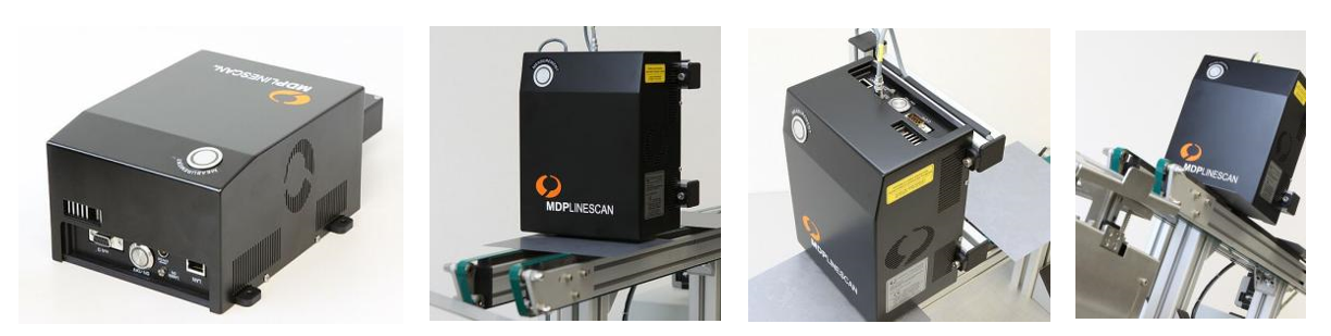
MDPlinescan is designed as an easy to integrate OEM device that can be integrated into various automated inspection lines. The key is to perform minority carrier lifetime scanning during the transmission process. The sample is usually carried by a conveyor belt or robot system under the measuring head. Application examples include testing from crystal bricks to wafers, single crystal minority carrier lifetime testing, polycrystalline minority carrier lifetime testing, with a measurement speed of less than one second per wafer. The incoming material quality inspection on the battery production line is a classic and universal case, also used for process quality inspection after passivation and diffusion, and has many other special application possibilities. Easy to integrate, only requiring Ethernet connection and power supply.
MDPlinescanW
Includes an additional resistivity measurement option.
Advantages:
◇Scanning minority carrier lifetime and resistivity under µ - PCD or steady-state excitation conditions is an important function of this small device;
◇OEMThe equipment can be integrated into the production line of polycrystalline or monocrystalline silicon wafers, at different preparation stages, up to devices, bricks, or ingots.
◇The compact size and standard automation interface make it easy to integrate. The focus is on the long-term reliability and accuracy of the measurement results.
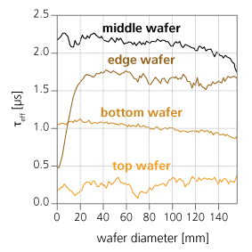
Demonstration line scan image
Details:
◇ Allow investigation of single crystal wafers
◇Different wafer levels have different formulas
◇Monitor material, process quality, and stability
Technical specifications:
| sample |
Multiple sizes of polycrystalline or monocrystalline wafers, such as 156mm × 156mm, crystal bricks, battery cells, etc |
| Sample size |
50 x 50 mm ² more than |
| resistivity |
0.2-10 ³ Ω · cm |
| Conductivity type |
P. N |
| Sample type |
Silicon wafers, partially or fully processed silicon wafers, compound semiconductors, and more products |
| Measurable characteristics |
Minority carrier lifetime |
| hardware interface |
Ethernet |
| Size specifications |
Volume: 174 x 107 x 205mm; Weight: 3 kilograms |
| source |
24 V DC, 2 A |