MDPspot W
Includes an additional resistivity measurement option. Measuring the resistivity of silicon can be used for wafers or bricks with no possibility of height adjustment. One of these two options must be predefined in advance.
|
|
|
|
Features:
◇ Contactless and non-destructive electrical semiconductor characteristics
◇include μ- PCD measurement options
◇Advanced sensitivity in visualizing invisible defects and studying epitaxial layers to date
◇Integrate up to four lasers for a wide injection horizontal range
◇Obtain raw data for a single transient and a map for special evaluation purposes
Technical specifications:
Single crystal or polycrystalline wafers, crystal bricks, batteries, silicon wafers, passivated or diffused wafers after different production steps |
|
Sample size |
50 x 50 mm² Above 12 "or 210 x 210 mm ² |
resistivity |
0.2-10³ Ω · cm |
material |
Chips, bricks, partially or completely processed silicon wafers, compound semiconductors, etc |
Measurement parameters |
Carrier lifetime |
size |
360 x 360 x 520 mm,Weight: 16 kg |
power |
110/220 V, 50/60 Hz, 3 A |
Advantages:
◇ Desktop device, used for single point measurement of carrier lifetime, polycrystalline silicon or monocrystalline silicon in different preparation stages, from raw materials to devices.
◇ Small size, low cost, and convenient to use. Comes with a basic software for small-scale applicationsPCOr visualize the results on a laptop.
Suitable for silicon wafers to bricks, with convenient height adjustment for operation.
Details:
◇Allow single crystal wafer investigation
◇Different wafer levels have different formulas
◇Monitor material, process quality, and stability
Additional options:
◇Spot size variation
◇Resistivity measurement (chip)
◇Background/Bias Light
◇Reflection measurement (MDP)
◇Software extension
◇Additional laser options
MDPspot application:
Iron concentration determination
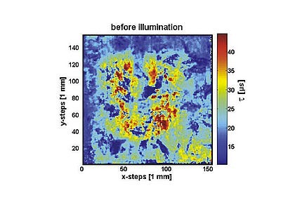
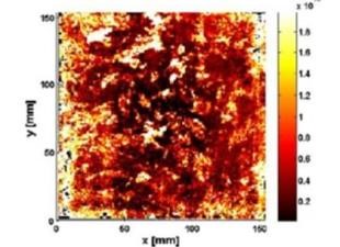
Accurate determination of iron concentration is crucial, as iron is one of the abundant and harmful defects in silicon. Therefore, it is necessary to measure iron concentration as accurately and quickly as possible, with very high resolution and * * being online
More
Doped samplePhotoconductivity measurement
The doping of B and P has many applications in the microelectronics industry, but so far, there is no method to check these without touching the sample and changing its properties due to necessary annealing stepsUniformity of doping. The difficulties so far
More
Trap concentration measurement
The trap center is very important, and in order to understand the behavior of charge carriers in materials, it can also have an impact on solar cells. Therefore, it is necessary to measure the center of these traps at high resolutionTrap densityandactivation energy.
More
Injection related measurements
The lifetime of minority carriers strongly depends on injection (excess residual carrier concentration). Doping can be inferred from the shape and height of the lifetime curveComposite CenterandCapture CenterInformation about.
More